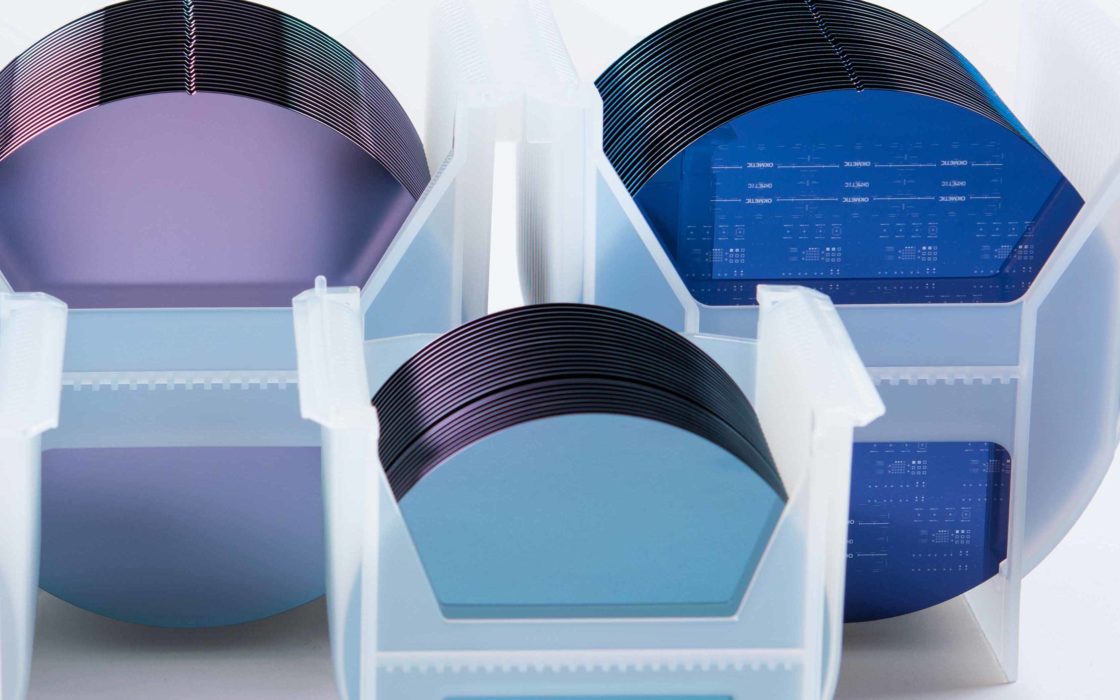
The Silicon on Insulator Market revenues were estimated at US$ 1.3 Billion in 2022 and is anticipated to grow at a CAGR of 14.3% from 2022 to 2032, according to a recently published Future Market Insights report. By the end of 2032, the market is expected to reach a valuation of US$ 4.9 Billion.
The key factors that are propelling Silicon on Insulator demand are the increasing use of SOI wafer-based technology in the automotive sector. For chipmakers in the automotive industry, the growing investments in ADAS and driverless automobiles have created enormous growth prospects. In the worldwide chip market, the automotive industry has had a substantial growth rate.
New features and an increase in the use of sensors, together with recent developments in the automobile industry, are fuelling the SOI market’s expansion. For instance, high-speed, low-power, small electrical equipment are needed to operate ADAS and driverless cars. As a result, SOI wafers are used to suffice these needs.
Download our Sample Report to Discover How Recent Industry Developments @
https://www.futuremarketinsights.com/reports/sample/rep-gb-15651
High-voltage and low-voltage components may be combined on a single chip using the SOI wafer, which would save space and money, simplify designs and models, improve performance, save development costs, and shorten the time to market. Additionally, SOI offers new approaches for well-established technologies like IoT, AI, and ML.
Additionally, planar semiconductor devices with better body distortion capabilities can be scaled up owing to FD-SOI semiconductor technology. For automotive applications, FD-SOI technology provides maximum energy efficiency, the highest integrated RF performance, and improved integrated circuit dependability.
As a response to COVID-19, the semiconductor industry was compelled to mobilize rapidly and make choices that would have long-term consequences. Along the value chain, semiconductor companies work together with a number of partners and suppliers from different countries to provide raw materials, equipment, assembly, testing, and packaging.
Competitive Landscape
Players in the market are constantly developing improved analytical solutions as well as extending their product offerings. The companies in Silicon on Insulator are focused on their alliances, technology collaborations, and product launch strategies. The Tier 2 Players in the market are targeting to increase their Silicon on Insulator share.
Some of the recent developments in the Silicon on Insulator are:
- In August 2021, Utilizing the Cadence Virtuoso Design Platform and RF Solutions, Tower Semiconductor Ltd. and Cadence Design Systems, Inc. introduced a silicon-tested SP4T RF-SOI switch reference design flow. For the development of advanced 5G wireless, cable infrastructure, and automotive IC products, the reference design pipeline offers a quicker route to design completion.
- In June 2021, with the help of a contract signed with GLOBALFOUNDRIES, Global Wafers Co., Ltd. (GWC) will increase the production of 200mm silicon-on-insulator (SOI) wafers and introduce 300mm SOI manufacturing at its MEMC plant. The supply of GF silicon wafers coming from the US is increased by this deal.
Grow your profit margin with Future Market Insights – Buy the Report @
https://www.futuremarketinsights.com/checkout/15651
More Insights Available
Future Market Insights, in its new offering, presents an unbiased analysis of the Silicon on Insulator Market, presenting historical market data (2015-2021) and forecast statistics for the period of 2022-2032.
The study reveals extensive growth in Silicon on Insulator Market in terms of Thickness (Thin Film SOI Wafers and Thick Film SOI Wafers) of Wafer Size, (200 mm and Less than 200 mm and 300 mm) of Wafer Type (RF-SOI, FD-SOI, PD-SOI, Power-SOI and Emerging-SOI), of Technology (Smart Cut, Bonding SOI and Layer Transfer SOI), of Product (RF FEM Products, MEMS Devices, Power Products, Optical Communication and Image Sensing), of Application (Consumer Electronics, Automotive, Datacom & Telecom, Industrial, Military, Defense, and Aerospace) of five regions (North America, Latin America, Europe, Asia Pacific and Middle East & Africa).
Silicon on Insulator Segmentation
By Thickness:
- Thin Film SOI Wafers
- Thick Film SOI Wafers
By Wafer Size:
- 200 mm and Less than 200 mm
- 300 mm
By Wafer Type:
- RF-SOI
- FD-SOI
- PD-SOI
- Power-SOI
- Emerging-SOI
By Technology:
- Smart Cut
- Bonding SOI
- Layer Transfer SOI
By Product:
- RF FEM Products
- MEMS Devices
- Power Products
- Optical Communication
- Image Sensing
By Application:
- Consumer Electronics
- Automotive
- Datacom & Telecom
- Industrial
- Military, Defence, and Aerospace
By Region:
- North America
- Latin America
- Europe
- APAC
- MEA
About Us
Future Market Insights, Inc. (ESOMAR certified, Stevie Award – recipient market research organization and a member of Greater New York Chamber of Commerce) provides in-depth insights into governing factors elevating the demand in the market. It discloses opportunities that will favor the market growth in various segments on the basis of Source, Application, Sales Channel and End Use over the next 10-years.
Contact Us:
Future Market Insights Inc.
Christiana Corporate, 200 Continental Drive,
Suite 401, Newark, Delaware – 19713, USA
T: +1-845-579-5705
For Sales Enquiries: sales@futuremarketinsights.com
Browse Other Reports: https://www.futuremarketinsights.com/reports
LinkedIn| Twitter| Blogs
