In 2021, the global EUV lithography market was valued at approximately USD 4,648.6 million. Looking ahead to 2029, the market is anticipated to experience substantial growth, with a projected Compound Annual Growth Rate (CAGR) of 21.5%, reaching an estimated USD 22,978.6 million. EUV, or Extreme Ultraviolet, refers to the specific wavelength of light used in this advanced lithography process. The development of more sophisticated lithographic systems is a key driver behind the increasing adoption of EUV technology.
The EUV Lithography Market report by Future Market Insights—an ESOMAR Certified Market Research and Consulting Firm—provides a comprehensive analysis of the sector. This report covers essential aspects of the EUV lithography market, including key drivers, market size, and forecasts. It features detailed revenue and shipment segmentations, along with a ten-year outlook extending to 2029. The report also examines major industry players, their market presence, competitive dynamics, and regional trends.
The EUV lithography market is poised for significant expansion, driven by the push for miniaturization of integrated circuits and microchips, increasing demand for higher wafer production, and the ongoing growth of the semiconductor industry. As technology evolves to enhance performance and efficiency, the adoption of EUV lithography is becoming essential for achieving the high resolution required for advanced semiconductor manufacturing.
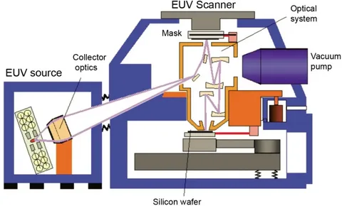
This technology plays a crucial role in semiconductor manufacturing, enabling the precise creation of complex patterns on silicon wafers. This process facilitates the production of smaller, faster, and more powerful semiconductors.
The future growth of the EUV lithography market is closely linked to continued advancements in chip manufacturing technology, miniaturization of integrated circuits, and increased wafer production scales. Despite high upfront costs and the nascent stage of the technology, ongoing innovation and research and development are expected to make EUV lithography more efficient and cost-effective. As a result, the market is projected to achieve a notable CAGR of 21.5% from 2022 to 2029, highlighting its pivotal role in the future of semiconductor manufacturing.
Full Market Assessment: Comprehensive Report
Key Takeaways:
- Reduction of microchip sizes to incorporate them into shrinking semiconductors is one of the prime factors that resulted in the development of EUV lithography technology.
- Emergence of artificial intelligence (AI), machine learning, industrial IoT (IIoT), and autonomous driving has been driving miniaturization of microchips, subsequently creating the need for EUV lithography in chip manufacturing.
- Constant innovation, R&D, and retrofitting of installed systems to improve wafer production, are anticipated to remain key trends in the EUV lithography market.
- Integrated device manufacturers (IDM) and foundries are projected to create bulk of the demand for EUV lithography systems, as they are responsible for majority of the microchip and integrated circuit (IC) demand across industries.
- Acquisition of stakes in key technology-based companies to complement product development is anticipated to remain a prominent trend in the market.
Competitive Landscape
Key players in the EUV Lithography market are focusing on a data-centric approach with an aim of expanding their portfolio of technology solutions that address customer needs. Many key players are also using innovation to expand their product offerings to meet customer requirements. Players are aiming at research & development to develop new products.
For Instance:
- In Jan 2022, ASML and Intel Corporation announced the latest phase of their longstanding collaboration to advance cutting-edge semiconductor lithography technology.
- In April 2019, Taiwan Semiconductor Manufacturing Co. Ltd announced the expansion of the Open Innovation Platform ® (OIP) Cloud Alliance, with Mentor Graphics joining inaugural members Amazon Web Services, Cadence, Microsoft Azure, and Synopsys.
- In March 2019, Samsung Electronics developed a 3rd-generation 10-nanometer-class (1z-nm) eight-gigabit (GB) Double Data Rate 4 (DDR4) DRAM for the first time in the industry.
- In October 2019, SK Hynix developed 1Znm 16GB (Gigabits) DDR4 (Double Data Rate 4) DRAM. As 16 GB is the industry’s largest density for a single chip, the total memory capacity per wafer is also the largest of the existing DRAMs.
Key Players
- ASML
- Nikon
- Canon
- Carl Zeiss
- Toppan Printing
- NTT Advanced Technology
- Intel
- Samsung
- SK Hynix
- Toshiba
- TSMC
- Global Foundries
Global EUV Lithography Market by Category By End Use :
- Integrated Device Manufacturer (IDM)
- Foundry
- Memory
By Region:
- Americas
- EMEA
- Asia Pacific
About Future Market Insights (FMI)
Future Market Insights, Inc. (ESOMAR certified, recipient of the Stevie Award, and a member of the Greater New York Chamber of Commerce) offers profound insights into the driving factors that are boosting demand in the market. FMI stands as the leading global provider of market intelligence, advisory services, consulting, and events for the Packaging, Food and Beverage, Consumer Technology, Healthcare, Industrial, and Chemicals markets. With a vast team of 400 analysts worldwide, FMI provides global, regional, and local expertise on diverse domains and industry trends across more than 110 countries.
Contact Us:
Future Market Insights Inc.
Christiana Corporate, 200 Continental Drive,
Suite 401, Newark, Delaware – 19713, USA
T: +1-845-579-5705
For Sales Enquiries: sales@futuremarketinsights.com
Website: https://www.futuremarketinsights.com
LinkedIn| Twitter| Blogs | YouTube