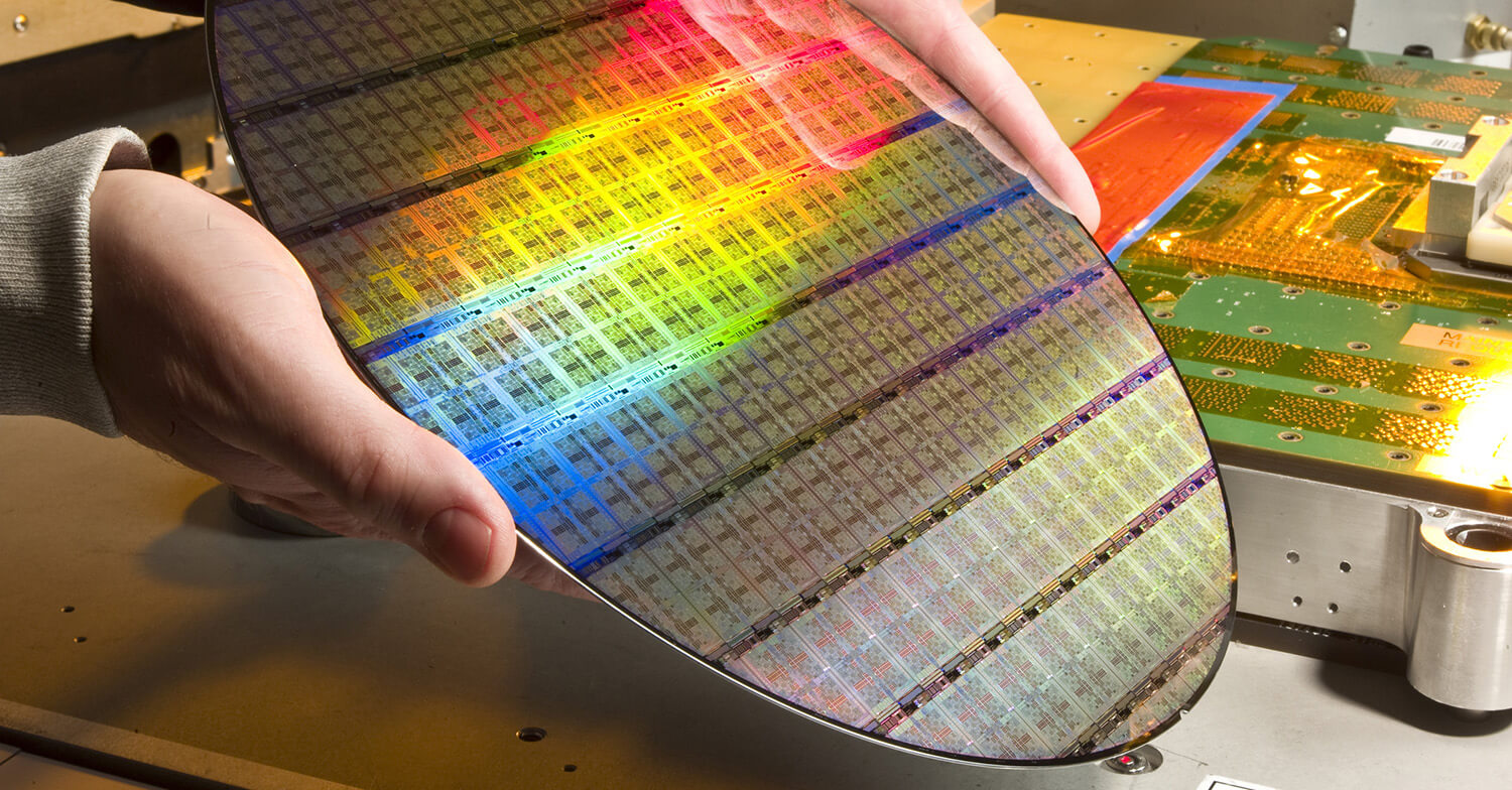
The semiconductor wafers market report, recently released by ESOMAR-certified market research firm Future Market Insights (FMI), forecasts a mostly positive growth trajectory for the 2020–2030 assessment period. The analysis reveals the key forces that will shape the market’s potential for future growth.
| Semiconductor Wafers Market Size (2022) | US$ 20.19 Bn |
| Sales Forecast (2030) | US$ 31.41 Bn |
| Global Market Growth Rate (2022 to 2030) | 5.7% CAGR |
| Share of Top 5 Market Players | 55% |
As businesses and corporations aim to diversify their operations in the future, one of the main growth drivers is the deeper adoption of 5G technology. A quarter of all mobile traffic data will be transmitted over 5G networks by 2024, which will be spread across 2/5 of the planet. As a result, wafer output to make ICs for 5G devices is increasing.
Get a Sample Copy of Report@
https://www.futuremarketinsights.com/reports/sample/rep-gb-12824
Key Takeaways
- By application, automotive semiconductor wafer to experience nearly twofold growth until 2030
- Extensive applications to be witnessed across consumer electronics, particularly in the manufacturing of integrated circuits (ICs)
- By size, 150-200 mm semiconductor wafers is likely to generate over 2/3rd revenue share by 2020-end
- East Asia to emerge as the market hegemon, with China pivoting maximum growth, Europe and North America remain highly lucrative
- Global semiconductor wafers market to register value CAGR worth 5.6% through 2030
COVID-19 Impact Analysis
The novel coronavirus pandemic has ushered in multiple impacts across the global semiconductor wafers market. Stringent government-mandated lockdowns have contracted production of automotives, a key application area for semiconductor wafers.
A 16% decline was experienced in the global automotive industry since the past few months, thereby restraining sales of semiconductor wafers for multiple purposes such as infotainment systems, collision detection and navigation.
Simultaneously, surging sales of consumer electronic products is keeping the semiconductor wafers market demand afloat, particularly across emerging economies. With mandatory lockdowns imposed, corporate entities, educational institutions and entertainment houses are encouraging virtual interactions, thus upscaling demand for smartphones, tablets and laptops.
Competitive Landscape
Prominent semiconductor wafers manufacturers profiled in the report include Applied Materials Inc., ASM International, Nikon Corporation, SCREEN Semiconductor Solutions Co. Ltd., Hitachi High-Technologies Corporation, Tokyo Electron Limited, ASML Holding N.V., KLA Corporation, Lam Research Corporation and others.
In November 2020, Hitachi High-Technologies Corporation launched its 3D SEM CT1000 used for defect observation across semiconductors. The devices enables a three-dimensional observation of pattern and defects shapes occurring during the manufacturing process on wafers measuring upto 200 mm in diameter.
Ask for Customization@
https://www.futuremarketinsights.com/customization-available/rep-gb-12824
Semiconductor Wafers Industry SurveySemiconductor Wafers Market by Wafer Size:
- Less than 150 mm Semiconductor Wafers
- 150 to 200 mm Semiconductor Wafers
- More than 200 mm Semiconductor Wafers
Semiconductor Wafers Market by Application:
- Automotive
- Consumer Electronics
- Industrial Manufacturing
- Telecommunications
- Others
Semiconductor Wafers Market by Region:
- North America Semiconductor Wafers Market
- Latin America Semiconductor Wafers Market
- Europe Semiconductor Wafers Market
- East Asia Semiconductor Wafers Market
- South Asia & Pacific Semiconductor Wafers Market
- Middle East & Africa (MEA) Semiconductor Wafers Market
Read Related Reports:
https://degentevakana.com/blogs/view/104288
https://ourclass.mn.co/posts/26911770
https://www.dronepilotlari.com/blogs/52340/Green-Technology-And-Sustainability-Market-2022-Key-Players-SWOT-Analysis
https://inobee.com/read-blog/90264
About FMI
Future Market Insights (ESOMAR certified market research organization and a member of Greater New York Chamber of Commerce) provides in-depth insights into governing factors elevating the demand in the market. It discloses opportunities that will favor the market growth in various segments on the basis of Source, Application, Sales Channel and End Use over the next 10-years.
Contact:
Future Market Insights Inc.
Christiana Corporate, 200 Continental Drive,
Suite 401, Newark, Delaware – 19713, USA
T: +1-845-579-5705
Report: https://www.futuremarketinsights.com/reports/semiconductor-wafers-market
For Sales Enquiries: sales@futuremarketinsights.com
Browse latest Market Reports: https://www.futuremarketinsights.com/reports
LinkedIn| Twitter| Blogs
